Laser Debonding Equipment Market to Reach USD 6.03 Billion by 2036 Amid Rising Advanced Semiconductor Packaging Demand
Semiconductor wafer debonding technology
The global Laser Debonding Equipment Market is gaining substantial momentum as semiconductor manufacturers increasingly invest in advanced packaging technologies, AI chip manufacturing, heterogeneous integration, and wafer-level processing solutions.
Laser debonding equipment has become an essential technology in modern semiconductor fabrication due to its ability to safely separate temporarily bonded wafers without damaging sensitive substrates. As the electronics industry continues to move toward ultra-thin wafers, chiplet architectures, 3D IC packaging, flexible displays, and high-performance semiconductor devices, the demand for precision laser debonding systems is increasing rapidly.
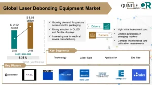
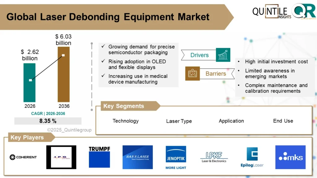
According to recent industry analysis by Quintile Reports, the global Laser Debonding Equipment Market is estimated at USD 2.62 billion in 2026 and is projected to reach approximately USD 6.03 billion by 2036, expanding at a CAGR of 8.35% during the forecast period.
The increasing adoption of advanced semiconductor packaging technologies, fan-out wafer-level packaging (FOWLP), temporary wafer bonding systems, and high-precision manufacturing processes is expected to drive long-term market growth.
Download Free Sample PDF of the Report https://www.quintilereports.com/request-sample/1296-laser-debonding-equipment-market/
What is Laser Debonding Equipment?
Laser debonding equipment is a high-precision manufacturing solution used to separate temporarily bonded wafers, substrates, OLED panels, micro-LED assemblies, and delicate semiconductor components using controlled laser energy.
Unlike traditional mechanical or chemical separation methods, laser debonding technology offers:
- Non-contact processing
- Reduced wafer damage
- Higher precision
- Improved manufacturing yield
- Lower contamination risk
- Better process consistency
The technology is widely used in advanced semiconductor packaging applications where precision and substrate integrity are critical.
Laser debonding systems are increasingly being integrated into semiconductor manufacturing equipment and automated smart factory environments to support large-scale electronics production.
Key Market Highlights
| Market Insights | Details |
| Market Size (2026) | USD 2.62 Billion |
| Projected Market Size (2036) | USD 6.03 Billion |
| CAGR (2026–2036) | 8.35% |
| Fastest Growing Region | Asia Pacific |
| Leading Application | Semiconductor Wafer Debonding |
| Major Growth Driver | Advanced Semiconductor Packaging |
Key Drivers Fueling the Laser Debonding Equipment Market
Rising Demand for Advanced Semiconductor Packaging
The semiconductor industry is rapidly transitioning toward advanced packaging technologies such as:
- Fan-Out Wafer-Level Packaging (FOWLP)
- 3D IC Packaging
- Chiplet-Based Architectures
- Heterogeneous Integration
- System-in-Package (SiP)
These next-generation packaging technologies require ultra-thin wafer processing and highly accurate temporary wafer bonding and debonding systems.
Laser debonding equipment enables manufacturers to separate wafers safely while minimizing stress, cracking, and yield loss.
The growing complexity of semiconductor devices is expected to significantly boost demand for laser debonding technology throughout the forecast period.
LinkedIn Article : https://www.linkedin.com/pulse/laser-debonding-equipment-market-set-reach-usd-603-billion-narayan-szmff
Growing AI and High-Performance Computing Semiconductor Demand
The rapid expansion of artificial intelligence (AI), machine learning, cloud computing, and high-performance computing (HPC) applications is driving demand for more powerful semiconductor chips.
To meet performance and miniaturization requirements, semiconductor manufacturers are increasingly adopting:
- Advanced wafer stacking
- 3D integration
- High-density interconnect technologies
- Precision wafer handling systems
Laser debonding systems play a critical role in supporting these advanced semiconductor manufacturing processes.
Increasing Adoption in OLED and Micro-LED Manufacturing
Flexible displays, foldable smartphones, automotive displays, and next-generation television technologies are accelerating demand for OLED and micro-LED manufacturing.
Laser debonding equipment allows manufacturers to process fragile display materials with minimal thermal and mechanical damage.
The technology improves production accuracy while reducing substrate breakage during manufacturing.
Focus on Sustainable and Low-Waste Manufacturing
Sustainability and yield optimization are becoming increasingly important in semiconductor manufacturing.
Compared to conventional chemical and mechanical separation methods, laser debonding technology provides:
- Reduced chemical waste
- Lower material loss
- Higher production efficiency
- Reduced consumable usage
- Cleaner manufacturing processes
As environmental regulations continue to strengthen globally, manufacturers are expected to invest more heavily in energy-efficient and eco-friendly semiconductor manufacturing technologies.
Technology Trends in the Laser Debonding Equipment Market
The Laser Debonding Equipment Market is evolving rapidly due to ongoing innovations in photonics, automation, and laser engineering.
Major Technologies Include:
- Laser-Induced Breakdown Spectroscopy (LIBS)
- Laser Ablation
- Laser-Induced Forward Transfer (LIFT)
- Photothermal Debonding Techniques
- Photochemical Debonding Technologies
Modern systems increasingly utilize:
- UV lasers
- Excimer lasers
- Infrared lasers
- Femtosecond lasers
- AI-driven process automation
- Robotic integration
These innovations improve throughput, precision, operational flexibility, and manufacturing scalability.
Latest Blog : https://www.researcheditorial.com/news/chiral-chromatography-columns-market/
Laser Debonding Equipment Market Segmentation
By Technology
- Laser-induced breakdown spectroscopy
- Laser ablation
- Laser-induced forward transfer
- Photothermal debonding techniques
- Photochemical debonding technologies
By Laser Type
- Ultraviolet (UV) laser
- Infrared (IR) laser
- Pulsed laser
- Fiber lasers
- CO lasers
By Application
- Semiconductor wafer debonding
- Solar cell interconnect debonding
- Medical device debonding
- Adhesive removal in automotive
- Battery recycling
By End-Use Industry
- Electronics and semiconductor
- Automotive
- Renewable energy and batteries
- Aerospace
- Medical devices
Regional Analysis of the Laser Debonding Equipment Market
North America
North America currently dominates the global Laser Debonding Equipment Market due to:
- Strong semiconductor infrastructure
- Government semiconductor investments
- U.S. CHIPS Act support
- High R&D spending
- Advanced manufacturing ecosystem
The region continues to witness increasing adoption across semiconductor packaging, medical devices, and automotive electronics manufacturing.
Asia Pacific
Asia Pacific is expected to register the fastest market growth during the forecast period.
Countries driving growth include:
- China
- Taiwan
- South Korea
- Japan
- India
These countries are heavily investing in semiconductor self-sufficiency, advanced packaging ecosystems, wafer fabrication, and smart manufacturing technologies.
Taiwan and South Korea are particularly important due to the presence of major semiconductor foundries and OSAT providers.
Europe
Europe continues to strengthen its position in the laser debonding equipment industry through strong automotive electronics manufacturing, renewable energy investments, and precision engineering expertise.
Germany remains a major innovation hub for industrial laser technologies and semiconductor manufacturing solutions.
Competitive Landscape
The Laser Debonding Equipment Market is highly competitive and innovation-driven.
Major companies are focusing on:
- Precision laser control
- Automation integration
- Smart factory compatibility
- High-throughput manufacturing
- Sustainability-focused solutions
- AI-enabled manufacturing optimization
Leading Companies in the Laser Debonding Equipment Market
- Coherent, Inc.
- IPG Photonics Corporation
- TRUMPF GmbH + Co. KG
- Hans Laser Technology Group
- Jenoptik AG
- LPKF Laser & Electronics AG
- MKS Instruments
- Universal Laser Systems
- Optomec
- Keyence Corporation
Challenges in the Laser Debonding Equipment Market
Despite strong growth opportunities, several challenges continue to impact market expansion.
High Initial Equipment Cost
Advanced laser debonding systems require substantial capital investment, limiting adoption among small and medium-sized manufacturers.
Technical Complexity
Different substrate materials and adhesive compositions require precise optimization of laser parameters, increasing process complexity.
Thermal Sensitivity Risks
Certain delicate materials remain vulnerable to overheating, warping, or incomplete separation during debonding.
Competition from Alternative Technologies
Mechanical, thermal, and chemical separation methods continue to compete in cost-sensitive manufacturing applications.
Future Outlook of the Laser Debonding Equipment Industry
The future outlook for the Laser Debonding Equipment Market remains highly positive as semiconductor manufacturers continue investing in advanced packaging technologies and next-generation chip manufacturing.
The increasing demand for:
- AI processors
- Data center chips
- Electric vehicle electronics
- Flexible displays
- Micro-LED technologies
- Semiconductor miniaturization
will continue driving adoption of precision laser debonding solutions.
As automation, robotics, and smart factory integration expand across semiconductor fabrication facilities, laser debonding equipment is expected to become a core technology in advanced electronics manufacturing.
Frequently Asked Questions (FAQs)
What is laser debonding equipment?
Laser debonding equipment is used to separate temporarily bonded wafers or substrates using controlled laser energy while minimizing physical damage.
Why is laser debonding important in semiconductor manufacturing?
It enables safe handling of ultra-thin wafers and supports advanced semiconductor packaging technologies such as 3D IC packaging and fan-out wafer-level packaging.
Which industries use laser debonding systems?
Industries using laser debonding equipment include semiconductors, electronics, automotive, renewable energy, aerospace, and medical devices.
What is driving the Laser Debonding Equipment Market?
Key growth drivers include advanced semiconductor packaging, AI chip demand, OLED manufacturing, smart factory automation, and sustainability initiatives.
Which region is expected to grow fastest?
Asia Pacific is expected to witness the fastest growth due to strong semiconductor manufacturing investments in China, Taiwan, South Korea, and Japan.
What are the major challenges in the market?
Major challenges include high equipment costs, process complexity, thermal sensitivity issues, and competition from alternative debonding methods.
Conclusion
The Laser Debonding Equipment Market is becoming an increasingly important segment within the global semiconductor manufacturing ecosystem.
As advanced semiconductor packaging, AI chip production, and precision electronics manufacturing continue to evolve, the demand for high-performance wafer debonding systems is expected to grow significantly.
Manufacturers investing in automation, precision laser systems, and sustainable manufacturing technologies are likely to gain a strong competitive advantage in the coming years.
The market presents substantial opportunities for semiconductor equipment manufacturers, photonics companies, investors, and industrial automation providers through 2036.
Related Reports
About Quintile Reports
Quintile Reports delivers comprehensive market intelligence, competitive analysis, and strategic industry insights across semiconductor, electronics, healthcare, industrial automation, and emerging technology sectors.
For customized market research solutions and detailed industry reports, contact:
Email: sales@quintilereports.com
Website: https://www.quintilereports.com